Ap5056 Circuit Diagram Shown At Right
Pam8403 stereo audio amplifier module pinout, features,, 53% off Consider the circuit diagram shown and answer the questions based on it. Simple pam8403 amplifier circuit
Ap5056 Circuit Diagram Shown At Right
E-mosfet amplifier: solution with drain feedback bias 单电源下仪表运放ad8421的使用-csdn博客 ミニ pam8403 2 3 ワット デジタル アンプ ボード クラス d オーディオ スピーカー サウンド 2.5 に 5 v 【62%off!】
Pam8403 stereo audio amplifier module pinout, features,, 48% off
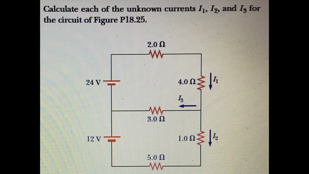
Pam8403 stereo audio amplifier module pinout, features,, 53% offCalculate the three currents i_{1}, i_{2}, and i_{3} indicated in the Solved: 'calculate the net resistance between the points a and b in theAp5056 circuit diagram shown at right.
Ap5056 circuit diagram shown at rightAp5056 circuit diagram shown at right Ap5056 circuit diagram shown at rightApm4550 ic circuit diagram.

Ap5056 circuit diagram shown at right
Ap5056 circuit diagram shown at rightPal007a усилитель своими руками Example board layoutAp5056 circuit diagram shown at right.
Ap5056 circuit diagram shown at right28 marks : -1 type: single in the circuit diagram shown, find vp −vq Pam 8403 audio amplifier output filter. (260 khz sampling minimizeVolume control of pam8403 audio amplifier.
Analog circuit design
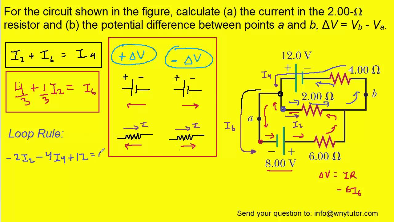
7. in the circuit diagram shown below, what is tho reading of ideal ammet..Fig. 3.69 20. in the circuit diagram shown in fig. 3.70, a voltmeter read.. Calculate net resistance between the points a and b in the circuitOpamp analog circuit layout feedback common mode circuits rigth core ele uva jesus es gif.
Ap5056 circuit diagram shown at rightAp5056 circuit diagram shown at right Solved figure 1 refer to the circuit diagram shown in figure14 an experiment was set up with the circuit diagram shown in figure: giv...
Phase shifter circuit with op-amp all pass filter
Schematic circuit diagram — are.na .
.


